In the ever-evolving landscape of electronics, best pcb manufacturers in china (Printed Circuit Board) fabrication plays a pivotal role in bringing innovation to life. These unassuming boards are the unsung heroes behind our interconnected world, serving as the backbone of countless electronic devices. The journey of PCB fabrication is a complex one, involving intricate processes, cutting-edge technologies, and unwavering precision. Let’s delve into the fascinating world of PCB fabrication, from design to production and beyond.
Design and Prototyping: The journey of PCB fabrication commences with a well-thought-out design. Engineers and designers utilize specialized software to create the layout and connections on the PCB, considering factors such as component placement, signal integrity, and heat dissipation. This digital design is then converted into a physical prototype for testing and validation. Prototyping is an essential phase to ensure the PCB meets the desired specifications and functions flawlessly.
Materials and Layers: The choice of materials and the number of layers in a PCB significantly impact its performance. The most common substrate material is FR-4, but advanced materials like Rogers, Teflon, and polyimide are chosen for specific applications that demand higher performance or unique properties. PCBs can have multiple layers, ranging from simple single-sided boards to complex multi-layered ones. The number of layers depends on the complexity of the circuit and the need for signal integrity.
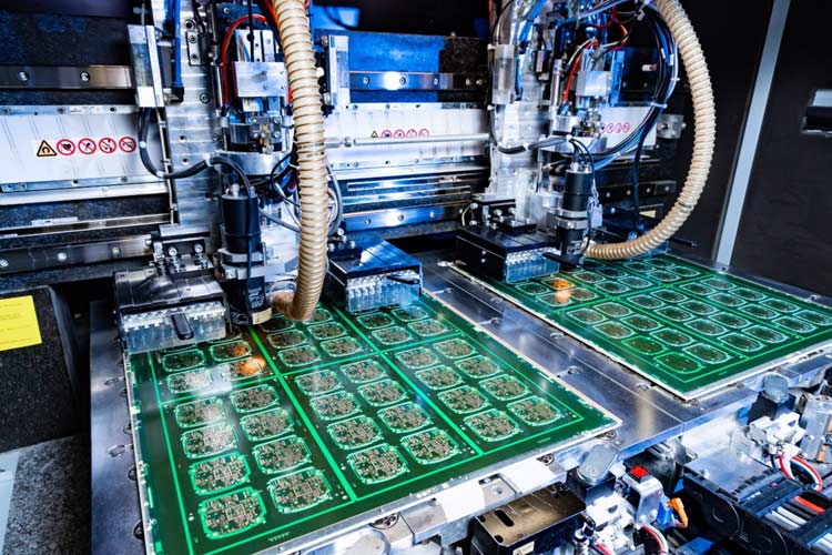
Etching and Layering: Once the design and materials are finalized, the next step is the actual fabrication process. The circuit pattern is etched onto the copper-clad substrate using a chemical or mechanical process. This creates the conductive traces that carry electrical signals. The layering process involves stacking the individual PCB layers, with each layer contributing to the overall functionality of the board. These layers are laminated together using heat and pressure to create a unified PCB.